1/19
March 2004
s
VERY LOW DROPOUT VOLTAGE (0.15V
TYP. AT 10mA LOAD)
s
LOW QUIESCENT CURRENT (TYP. 2.5mA,
AT 100mA LOAD)
s
OUTPUT CURRENT UP TO 100mA
s
ADJUSTABLE (FROM V
OUT
= 2.5V ONLY
SO-8) AND FIXED (3.3V & 5V) OUTPUT
VOLTAGE VERSION
s
INTERNAL CURRENT AND THERMAL LIMIT
s
LOAD DUMP PROTECTION UP TO 60V
s
REVERSE TRANSIENT PROTECTION UP
TO -50V
s
TEMPERATURE RANGE: -40 TO 125∞C
s
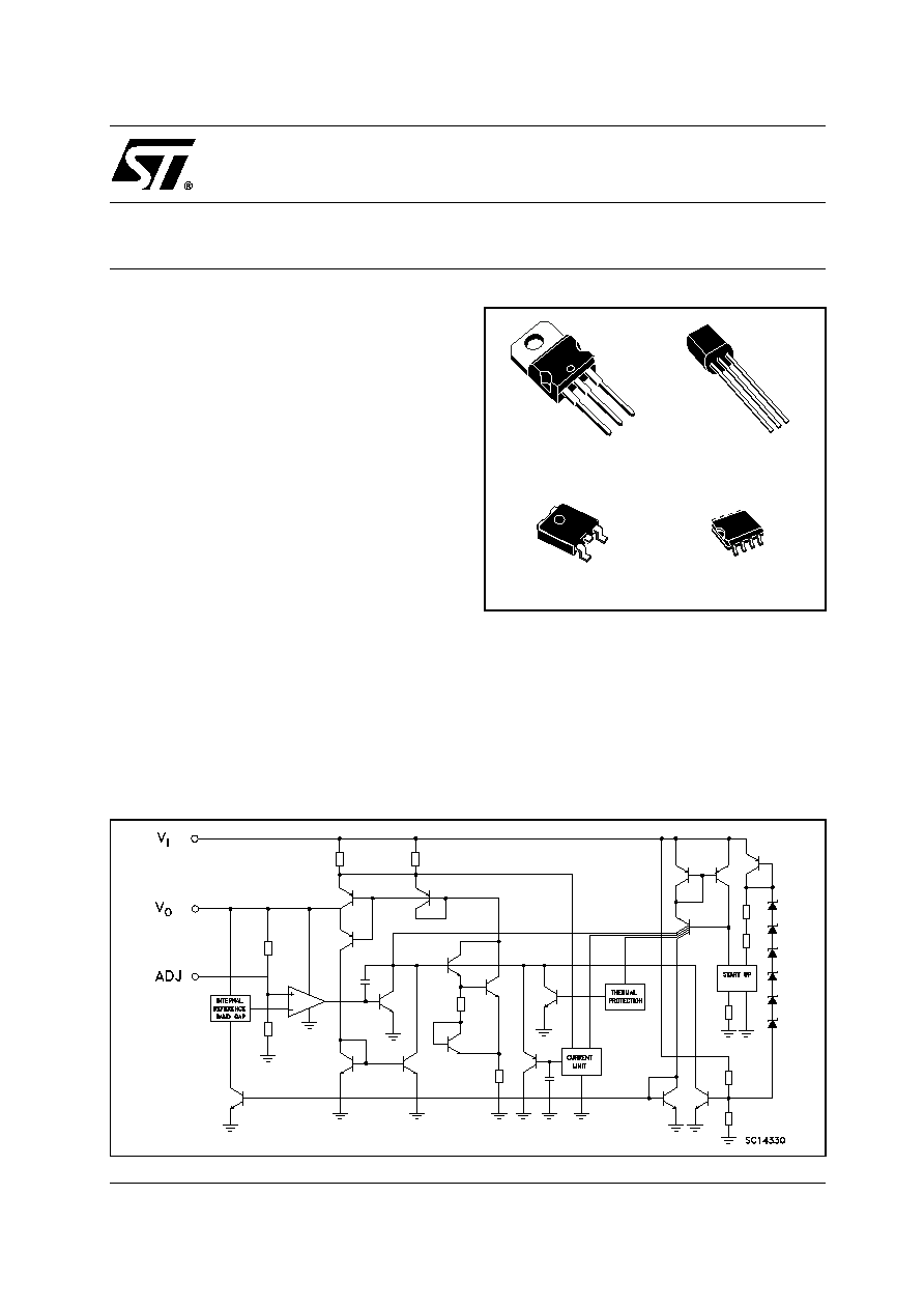
PACKAGE AVAILABLE: TO-92, DPAK,
TO-220, SO-8 (WITH INHIBIT CONTROL)
DESCRIPTION
The LM2931 series are very low drop regulators.
The very low drop voltage and the low quiescent
current make them particular suitable for low
noise, low power applications and in battery
powered systems. In the 8 pin configuration
(SO-8), fully compatible to the older L78L00
family, a shut down Logic Control function is
available.
This means that when the device is used as a
local regulator is possible to put a part of the board
in
stand-by
decreasing
the
total
power
consumption. Ideal for automotive application the
LM2931
is
protected
from
reverse
battery
installations or 2 battery jumps. During the
transient, such as a a load dump (60V) when the
input voltage can exceed the specified maximum
operating input voltage (26V), the regulator will
automatically shut down to protect both internal
circuit and the load.
LM2931
SERIES
VERY LOW DROP
VOLTAGE REGULATORS WITH INHIBIT FUNCTION
SCHEMATIC DIAGRAM
TO-220
SO-8
TO-92
DPAK
LM2931 SERIES
2/19
ABSOLUTE MAXIMUM RATINGS
Absolute Maximum Ratings are those values beyond which damage to the device may occur. Functional operation under these condition is
not implied.
THERMAL DATA
(*) Considering 6 cm
2
of copper board heat-sink
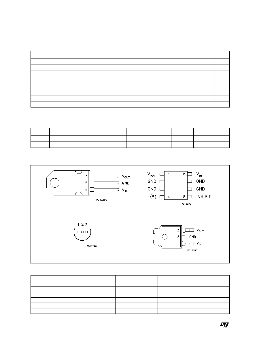
CONNECTION DIAGRAM (top view)
ORDERING CODES
(*) Available in Tape & Reel with the suffix "R" for fixed version and "-R" for adjustable version.
Symbol
Parameter
Value
Unit
V
I
DC Positive Input Voltage
40
V
V
I
DC Reverse Input Voltage
-15
V
V
I
Transient Input Voltage (
< 100ms)
60
V
V
I
Transient Reverse Input Voltage (
< 100ms)
-50
V
V
INH
Inhibit Input Voltage
40
V
I
O
Output Current
Internally Limited
T
stg
Storage Temperature Range
-65 to 150
∞C
T
op
Operating Junction Temperature Range
-40 to 125
∞C
Symbol
Parameter
TO-220
SO-8
DPAK
TO-92
Unit
R
thj-case
Thermal Resistance Junction-case
3
20
8
∞C/W
R
thj-amb
Thermal Resistance Junction-ambient
50
55(*)
100
200
∞C/W
TO-220
DPAK (*)
TO-92 (*)
SO-8 (*)
OUTPUT
VOLTAGE
LM2931AV33
LM2931ADT33
LM2931AZ33
LM2931AD33
3.3 V
LM2931BV33
LM2931BDT33
LM2931BZ33
LM2931BD33
3.3 V
LM2931AV50
LM2931ADT50
LM2931AZ50
LM2931AD50
5.0 V
LM2931BV50
LM2931BDT50
LM2931BZ50
LM2931BD50
5.0 V
LM2931D
2.5 to 26 V
TO-220
SO-8
DPAK
(*) = N.C. for FIXED and ADJ for ADJUSTABLE
TO-92
BOTTOM VIEW
PIN 1 = V
OUT
PIN 2 = GND
PIN 3 = V
IN
LM2931 SERIES
3/19
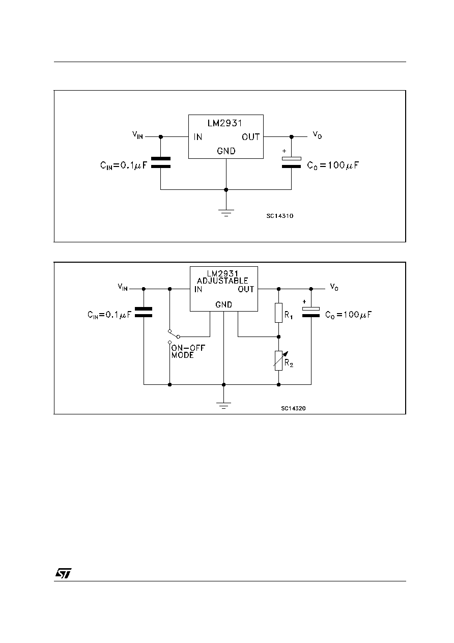
APPLICATION CIRCUIT FOR FIXED OUTPUT
APPLICATION CIRCUIT FOR ADJUSTABLE OUTPUT
R
1
suggested Value = 27K
V
O
= V
REF
(R
1
+ R
2
)/R
1
.

LM2931 SERIES
4/19
ELECTRICAL CHARACTERISTICS OF LM2931A 3.3V (refer to the test circuits, T
J
= 25∞C,
C
I
= 0.1 µF, C
O
= 100 µF, V
I
= 14V, I
O
= 10mA, V
INH
= 0V, unless otherwise specified).
Note 1: Reference Voltage is measured from V
OUT
to ADJ pin.
Note 2: V
d
measured when the output voltage has dropped 100mV from the nominal value obtained at 14V.
Symbol
Parameter
Test Conditions
Min.
Typ.
Max.
Unit
V
I
Maximum Operating Input
Voltage
I
O
= 10 mA
T
J
= -40 to 125∞C
26
37
V
V
O
Output Voltage
3.135
3.3
3.425
V
V
O
Output Voltage
I
O
= 100 mA V
I
= 6 to 26 V
T
J
= -40 to 125∞C
3.135
3.3
3.465
V
V
O
Line Regulation
V
I
= 9 to 16 V
2
10
mV
V
I
= 6 to 26 V
4
33
V
O
Load Regulation
I
O
= 5 to 100 mA
10
33
mV
V
d
Dropout Voltage (Note 1, 2) I
O
= 10 mA
90
250
mV
I
O
= 100 mA
250
600
I
d
Quiescent Current
ON MODE
I
O
= 100 mA
2.5
30
mA
OFF MODE
V
INH
= 2.5 V
R
LOAD
= 330
0.3
1
mA
I
SC
Short Circuit Current
100
300
mA
SVR
Supply Voltage Rejection
I
O
= 100 mA,
V
I
= 14 ± 2 V
f = 120 Hz,
T
J
= -40 to 125∞C
55
78
dB
V
IL
Control Input Voltage Low
T
J
= -40 to 125∞C
2
1.2
V
V
IH
Control Input Voltage High
T
J
= -40 to 125∞C
3.25
2
V
I
INH
Inhibit Input Current
V
INH
= 2.5 V
22
50
µA
V
I
Transient Input Voltage
R
LOAD
= 330
< 100ms
60
70
V
V
I
Reverse Polarity Input
Voltage
V
O
= ± 0.3 V
R
LOAD
= 330
-15
-50
V
V
I
Reverse Polarity Input
Voltage Transient
R
LOAD
= 330
< 100ms
-50
V
eN
Output Noise Voltage
B =10 Hz to 100 KHz
330
µ
V
RMS

LM2931 SERIES
5/19
ELECTRICAL CHARACTERISTICS OF LM2931B 3.3V (refer to the test circuits, T
J
= 25∞C,
C
I
= 0.1 µF, C
O
= 100 µF, V
I
= 14V, I
O
= 10mA, V
INH
= 0V, unless otherwise specified).
Note 1: Reference Voltage is measured from V
OUT
to ADJ pin.
Note 2: V
d
measured when the output voltage has dropped 100mV from the nominal value obtained at 14V.
Symbol
Parameter
Test Conditions
Min.
Typ.
Max.
Unit
V
I
Maximum Operating Input
Voltage
I
O
= 10 mA
T
J
= -40 to 125∞C
26
37
V
V
O
Output Voltage
3.135
3.3
3.465
V
V
O
Output Voltage
I
O
= 100 mA V
I
= 6 to 26 V
T
J
= -40 to 125∞C
2.97
3.3
3.63
V
V
O
Line Regulation
V
I
= 9 to 16 V
2
10
mV
V
I
= 6 to 26 V
4
33
V
O
Load Regulation
I
O
= 5 to 100 mA
10
33
mV
V
d
Dropout Voltage (Note 1, 2) I
O
= 10 mA
90
200
mV
I
O
= 100 mA
250
600
I
d
Quiescent Current
ON MODE
I
O
= 100 mA
2.5
30
mA
OFF MODE
V
INH
= 2.5 V
R
LOAD
= 330
0.3
1
mA
I
SC
Short Circuit Current
100
300
mA
SVR
Supply Voltage Rejection
I
O
= 100 mA,
V
I
= 14 ± 2 V
f = 120 Hz,
T
J
= -40 to 125∞C
55
78
dB
V
IL
Control Input Voltage Low
T
J
= -40 to 125∞C
2
1.2
V
V
IH
Control Input Voltage High
T
J
= -40 to 125∞C
3.25
2
V
I
INH
Inhibit Input Current
V
INH
= 2.5 V
22
50
µA
V
I
Transient Input Voltage
R
LOAD
= 330
< 100ms
60
70
V
V
I
Reverse Polarity Input
Voltage
V
O
= ± 0.3 V
R
LOAD
= 330
-15
-50
V
V
I
Reverse Polarity Input
Voltage Transient
R
LOAD
= 330
< 100ms
-50
V
eN
Output Noise Voltage
B =10 Hz to 100 KHz
330
µ
V
RMS
LM2931 SERIES
6/19
ELECTRICAL CHARACTERISTICS OF LM2931A 5V (refer to the test circuits, T
J
= 25∞C,
C
I
= 0.1 µF, C
O
= 100 µF, V
I
= 14V, I
O
= 10mA, V
INH
= 0V, unless otherwise specified).
Note 1: Reference Voltage is measured from V
OUT
to ADJ pin.
Note 2: V
d
measured when the output voltage has dropped 100mV from the nominal value obtained at 14V.
Symbol
Parameter
Test Conditions
Min.
Typ.
Max.
Unit
V
I
Maximum Operating Input
Voltage
I
O
= 10 mA
T
J
= -40 to 125∞C
26
37
V
V
O
Output Voltage
4.81
5
5.19
V
V
O
Output Voltage
I
O
= 100 mA V
I
= 6 to 26 V
T
J
= -40 to 125∞C
4.75
5
5.25
V
V
O
Line Regulation
V
I
= 9 to 16 V
2
10
mV
V
I
= 6 to 26 V
4
30
V
O
Load Regulation
I
O
= 5 to 100 mA
15
50
mV
V
d
Dropout Voltage (Note 1, 2) I
O
= 10 mA
90
200
mV
I
O
= 100 mA
250
600
I
d
Quiescent Current
ON MODE
I
O
= 100 mA
2.5
30
mA
OFF MODE
V
INH
= 2.5 V
R
LOAD
= 500
0.3
1
mA
I
SC
Short Circuit Current
100
300
mA
SVR
Supply Voltage Rejection
I
O
= 100 mA,
V
I
= 14 ± 2 V
f = 120 Hz,
T
J
= -40 to 125∞C
55
75
dB
V
IL
Control Input Voltage Low
T
J
= -40 to 125∞C
2
1.2
V
V
IH
Control Input Voltage High
T
J
= -40 to 125∞C
3.25
2
V
I
INH
Inhibit Input Current
V
INH
= 2.5 V
22
50
µA
V
I
Transient Input Voltage
R
LOAD
= 500
< 100ms
60
70
V
V
I
Reverse Polarity Input
Voltage
V
O
= ± 0.3 V
R
LOAD
= 500
-15
-50
V
V
I
Reverse Polarity Input
Voltage Transient
R
LOAD
= 500
< 100ms
-50
V
eN
Output Noise Voltage
B =10 Hz to 100 KHz
500
µ
V
RMS
LM2931 SERIES
7/19
ELECTRICAL CHARACTERISTICS OF LM2931B 5V (refer to the test circuits, T
J
= 25∞C,
C
I
= 0.1 µF, C
O
= 100 µF, V
I
= 14V, I
O
= 10mA, V
INH
= 0V, unless otherwise specified).
Note 1: Reference Voltage is measured from V
OUT
to ADJ pin.
Note 2: V
d
measured when the output voltage has dropped 100mV from the nominal value obtained at 14V.
Symbol
Parameter
Test Conditions
Min.
Typ.
Max.
Unit
V
I
Maximum Operating Input
Voltage
I
O
= 10 mA
T
J
= -40 to 125∞C
26
37
V
V
O
Output Voltage
4.75
5
5.25
V
V
O
Output Voltage
I
O
= 100 mA V
I
= 6 to 26 V
T
J
= -40 to 125∞C
4.5
5
5.5
V
V
O
Line Regulation
V
I
= 9 to 16 V
2
10
mV
V
I
= 6 to 26 V
4
30
V
O
Load Regulation
I
O
= 5 to 100 mA
15
50
mV
V
d
Dropout Voltage (Note 1, 2) I
O
= 10 mA
90
200
mV
I
O
= 100 mA
250
600
I
d
Quiescent Current
ON MODE
I
O
= 100 mA
2.5
30
mA
OFF MODE
V
INH
= 2.5 V
R
LOAD
= 500
0.3
1
mA
I
SC
Short Circuit Current
100
300
mA
SVR
Supply Voltage Rejection
I
O
= 100 mA,
V
I
= 14 ± 2 V
f = 120 Hz,
T
J
= -40 to 125∞C
55
75
dB
V
IL
Control Input Voltage Low
T
J
= -40 to 125∞C
2
1.2
V
V
IH
Control Input Voltage High
T
J
= -40 to 125∞C
3.25
2
V
I
INH
Inhibit Input Current
V
INH
= 2.5 V
22
50
µA
V
I
Transient Input Voltage
R
LOAD
= 500
< 100ms
60
70
V
V
I
Reverse Polarity Input
Voltage
V
O
= ± 0.3 V
R
LOAD
= 500
-15
-50
V
V
I
Reverse Polarity Input
Voltage Transient
R
LOAD
= 500
< 100ms
-50
V
eN
Output Noise Voltage
B =10 Hz to 100 KHz
500
µ
V
RMS
LM2931 SERIES
8/19
ELECTRICAL CHARACTERISTICS OF LM2931ADJ (refer to the test circuits figure 2 with R
1
= 27K
and R
2
= 40.5K
, T
J
= 25∞C, C
I
= 0.1 µF, C
O
= 100 µF, V
I
= 14V, I
O
= 10mA, V
INH
= 0V, unless otherwise
specified).
Note 1: Reference Voltage is measured from V
OUT
to ADJ pin.
Note 2: V
d
measured when the output voltage has dropped 100mV from the nominal value obtained at 14V.
Symbol
Parameter
Test Conditions
Min.
Typ.
Max.
Unit
V
I
Maximum Operating Input
Voltage
I
O
= 10 mA
T
J
= -40 to 125∞C
26
37
V
V
REF
Reference Voltage (Note 1)
1.14
1.2
1.26
V
V
REF
Reference Voltage (Note 1) I
O
= 100 mA
T
J
= -40 to 125∞C
1.08
1.2
1.32
V
V
O
Line Regulation
V
I
= 3.6 to 26 V
0.6
4.5
mV
V
O
Load Regulation
I
O
= 5 to 100 mA
9
30
mV
V
d
Dropout Voltage (Note 1, 2) I
O
= 10 mA
90
200
mV
I
O
= 100 mA
250
600
I
d
Quiescent Current
ON MODE
I
O
= 100 mA
2.5
30
mA
OFF MODE
V
INH
= 2.5 V
R
LOAD
= 300
0.3
1
mA
I
SC
Short Circuit Current
100
300
mA
SVR
Supply Voltage Rejection
I
O
= 100 mA
V
I
= 14 ± 2 V
f = 120 Hz
T
J
= -40 to 125∞C
55
80
dB
V
IL
Control Input Voltage Low
T
J
= -40 to 125∞C
2
1.2
V
V
IH
Control Input Voltage High
T
J
= -40 to 125∞C
3.25
2
V
I
INH
Inhibit Input Current
V
INH
= 2.5 V
22
50
µA
V
I
Transient Input Voltage
R
LOAD
= 300
< 100ms
60
70
V
V
I
Reverse Polarity Input
Voltage
V
O
= ± 0.3 V
R
LOAD
= 300
-15
-50
V
V
I
Reverse Polarity Input
Voltage Transient
R
LOAD
= 300
< 100ms
-50
V
eN
Output Noise Voltage
B =10 Hz to 100 KHz
330
µ
V
RMS
LM2931 SERIES
9/19
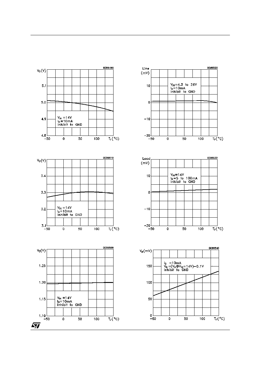
TYPICAL CHARACTERISTICS (unless otherwise specified C
I
= 0.1 µF, C
O
= 100 µF).
Figure 1 : Output Voltage vs Temperature
Figure 2 : Output Voltage vs Temperature
Figure 3 : Reference Voltage vs Temperature
Figure 4 : Line Regulation vs Temperature
Figure 5 : Load Regulation vs Temperature
Figure 6 : Dropout Voltage vs Temperature
LM2931 SERIES
10/19
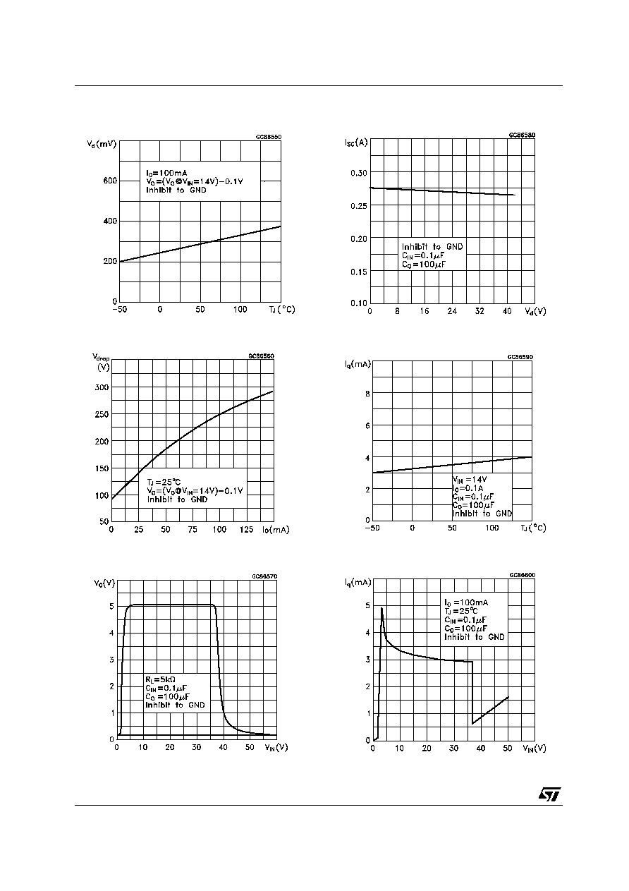
Figure 7 : Dropout Voltage vs Temperature
Figure 8 : Dropout Voltage vs Output Current
Figure 9 : Output Voltage vs Input Voltage
Figure 10 : Short Circuit Current vs Drop
Voltage
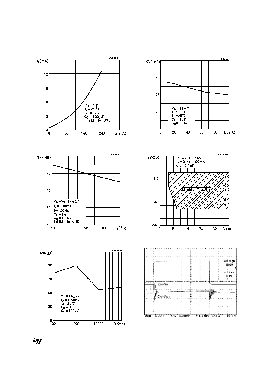
Figure 11 : Quiescent Current vs Temperature
Figure 12 : Quiescent Current vs Input Voltage
LM2931 SERIES
11/19
Figure 13 : Quiescent Current vs Output Current
Figure 14 : Supply Voltage Rejection vs
Temperature
Figure 15 : Supply Voltage Rejection vs
Frequency
Figure 16 : Supply Voltage Rejection vs
Output Current
Figure 17 : Stability vs C
O
Figure 18 : Line Transient
V
I
= 6 to 20 V, R
L
= 500
, T
J
= 25∞C, C
I
= 0, C
O
= 100µF,
Rise Fall-Time = 200 ns
LM2931 SERIES
12/19
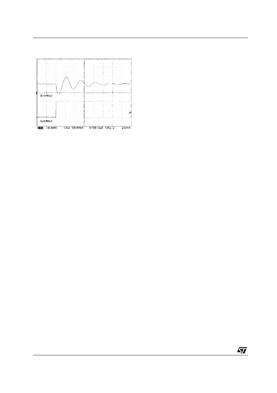
Figure 19 : Load Transient
V
I
= 14 V, I
O
= 100mA, T
J
= 25∞C, C
I
= 0.1µF, C
O
= 100µF,
Rise Time = 500ns, Fall-Time = 1µs
LM2931 SERIES
13/19
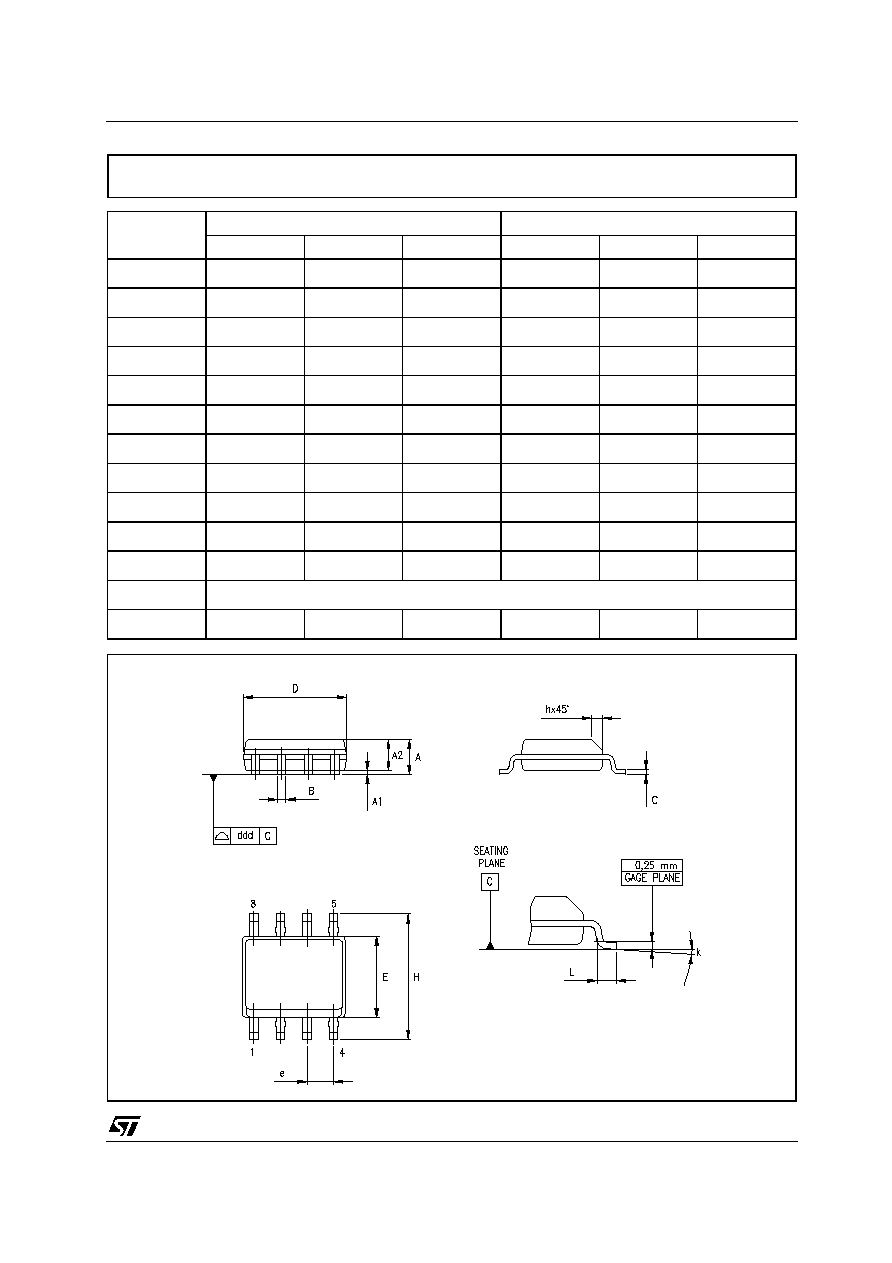
DIM.
mm.
inch
MIN.
TYP
MAX.
MIN.
TYP.
MAX.
A
4.40
4.60
0.173
0.181
C
1.23
1.32
0.048
0.051
D
2.40
2.72
0.094
0.107
D1
1.27
0.050
E
0.49
0.70
0.019
0.027
F
0.61
0.88
0.024
0.034
F1
1.14
1.70
0.044
0.067
F2
1.14
1.70
0.044
0.067
G
4.95
5.15
0.194
0.203
G1
2.4
2.7
0.094
0.106
H2
10.0
10.40
0.393
0.409
L2
16.4
0.645
L4
13.0
14.0
0.511
0.551
L5
2.65
2.95
0.104
0.116
L6
15.25
15.75
0.600
0.620
L7
6.2
6.6
0.244
0.260
L9
3.5
3.93
0.137
0.154
DIA.
3.75
3.85
0.147
0.151
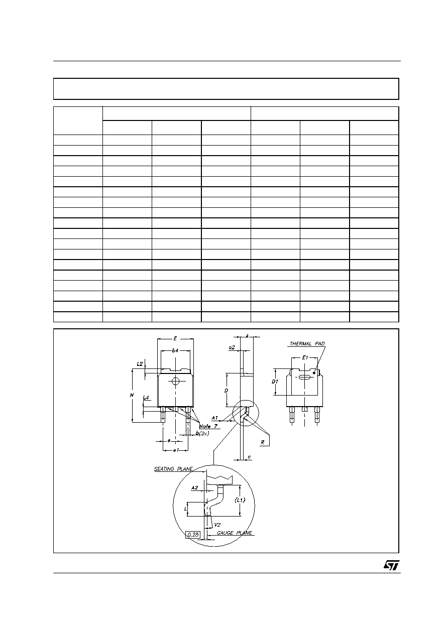
TO-220 MECHANICAL DATA
P011C
LM2931 SERIES
14/19
DIM.
mm.
mils
MIN.
TYP
MAX.
MIN.
TYP.
MAX.
A
4.32
4.95
170.1
194.9
b
0.36
0.51
14.2
20.1
D
4.45
4.95
175.2
194.9
E
3.30
3.94
129.9
155.1
e
2.41
2.67
94.9
105.1
e1
1.14
1.40
44.9
55.1
L
12.7
15.49
500.0
609.8
R
2.16
2.41
85.0
94.9
S1
0.92
1.52
36.2
59.8
W
0.41
0.56
16.1
22.0
TO-92 MECHANICA DATA
0102782/C
LM2931 SERIES
15/19
DIM.
mm.
inch
MIN.
TYP
MAX.
MIN.
TYP.
MAX.
A
1.35
1.75
0.053
0.069
A1
0.10
0.25
0.04
0.010
A2
1.10
1.65
0.043
0.065
B
0.33
0.51
0.013
0.020
C
0.19
0.25
0.007
0.010
D
4.80
5.00
0.189
0.197
E
3.80
4.00
0.150
0.157
e
1.27
0.050
H
5.80
6.20
0.228
0.244
h
0.25
0.50
0.010
0.020
L
0.40
1.27
0.016
0.050
k
∞ (max.)
ddd
0.1
0.04
SO-8 MECHANICAL DATA
0016023/C
8
LM2931 SERIES
16/19
DIM.
mm.
inch
MIN.
TYP
MAX.
MIN.
TYP.
MAX.
A
2.2
2.4
0.086
0.094
A1
0.9
1.1
0.035
0.043
A2
0.03
0.23
0.001
0.009
B
0.64
0.9
0.025
0.035
B2
5.2
5.4
0.204
0.212
C
0.45
0.6
0.017
0.023
C2
0.48
0.6
0.019
0.023
D
6
6.2
0.236
0.244
D1
5.1
0.200
E
6.4
6.6
0.252
0.260
E1
4.7
0.185
e
2.28
0.090
e1
4.4
4.6
0.173
0.181
H
9.35
10.1
0.368
0.397
L
1
0.039
(L1)
2.8
0.110
L2
0.8
0.031
L4
0.6
1
0.023
0.039
DPAK MECHANICAL DATA
0068772-F
LM2931 SERIES
17/19
DIM.
mm.
inch
MIN.
TYP
MAX.
MIN.
TYP.
MAX.
A
330
12.992
C
12.8
13.0
13.2
0.504
0.512
0.519
D
20.2
0.795
N
60
2.362
T
22.4
0.882
Ao
6.80
6.90
7.00
0.268
0.272
0.2.76
Bo
10.40
10.50
10.60
0.409
0.413
0.417
Ko
2.55
2.65
2.75
0.100
0.104
0.105
Po
3.9
4.0
4.1
0.153
0.157
0.161
P
7.9
8.0
8.1
0.311
0.315
0.319
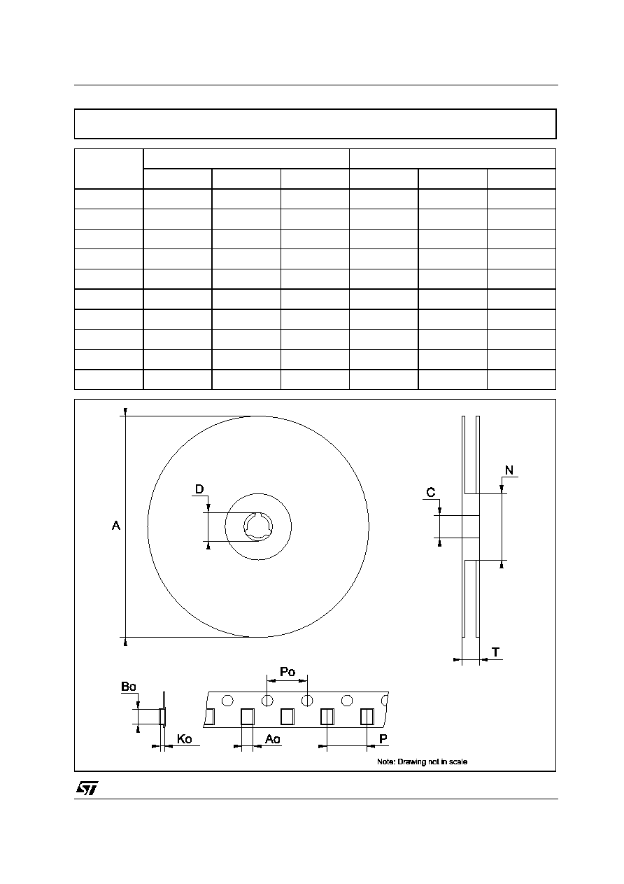
Tape & Reel DPAK-PPAK MECHANICAL DATA
LM2931 SERIES
18/19
DIM.
mm.
inch
MIN.
TYP
MAX.
MIN.
TYP.
MAX.
A
330
12.992
C
12.8
13.2
0.504
0.519
D
20.2
0.795
N
60
2.362
T
22.4
0.882
Ao
8.1
8.5
0.319
0.335
Bo
5.5
5.9
0.216
0.232
Ko
2.1
2.3
0.082
0.090
Po
3.9
4.1
0.153
0.161
P
7.9
8.1
0.311
0.319
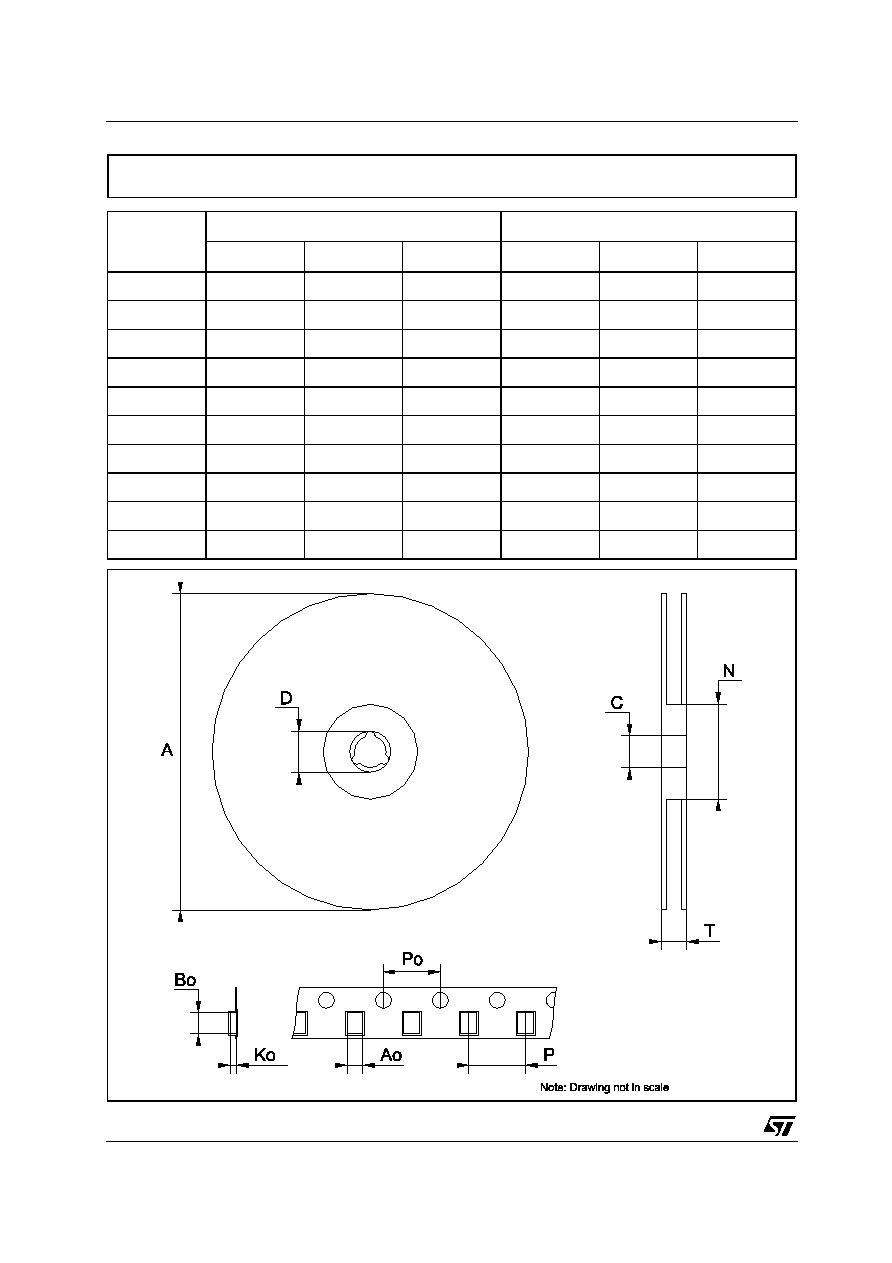
Tape & Reel SO-8 MECHANICAL DATA

LM2931 SERIES
19/19
Information furnished is believed to be accurate and reliable. However, STMicroelectronics assumes no responsibility for the
consequences of use of such information nor for any infringement of patents or other rights of third parties which may result from
its use. No license is granted by implication or otherwise under any patent or patent rights of STMicroelectronics. Specifications
mentioned in this publication are subject to change without notice. This publication supersedes and replaces all information
previously supplied. STMicroelectronics products are not authorized for use as critical components in life support devices or
systems without express written approval of STMicroelectronics.
The ST logo is a registered trademark of STMicroelectronics
All other names are the property of their respective owners
© 2004 STMicroelectronics - All Rights Reserved
STMicroelectronics GROUP OF COMPANIES
Australia - Belgium - Brazil - Canada - China - Czech Republic - Finland - France - Germany - Hong Kong - India - Israel - Italy - Japan -
Malaysia - Malta - Morocco - Singapore - Spain - Sweden - Switzerland - United Kingdom - United States.
http://www.st.com